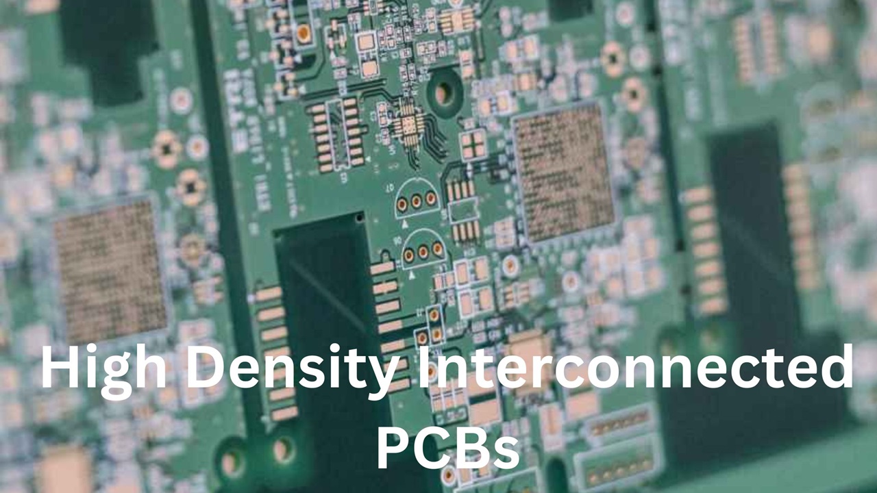
Choosing Printed Circuit Boards (PCBs) is vital in determining device performance, efficiency, and overall functionality in electronics design. Engineers constantly seek innovative solutions to meet these challenges as technology advances and demands for compact, high-performance electronics increase. One such solution gaining significant traction is High-Density Interconnected PCB or HDI PCB. Read on to delve into the top benefits of incorporating these into your designs.
Enhanced Design Flexibility
These circuit boards offer unparalleled design flexibility, allowing engineers to achieve more functionality within a smaller footprint. Unlike traditional PCBs, which have limitations in routing density and component placement, HDI technology enables the creation of complex, densely packed layouts with multiple routing layers. This enhanced flexibility empowers designers to optimize space utilization, reduce signal interference, and improve overall system performance.
Improved Signal Integrity
Signal integrity is paramount in high-speed electronic devices, where even minor disturbances can lead to signal degradation and performance issues. These circuit boards maintain integrity by minimizing loss, crosstalk, and electromagnetic interference. With shorter paths and reduced parasitic effects, HDI technology ensures reliable high-frequency data transmission, improving transfer rates and system stability.
Higher Component Density
The compact nature of these circuit panels allows for higher component density than conventional PCBs. By utilizing advanced manufacturing techniques such as micro vias, blind vias, and buried vias, engineers can densely pack components on multiple layers of the PCB, thereby maximizing functionality in a limited space. This increased component density enables the integration of more features, simplifies assembly, and reduces overall manufacturing costs.
Enhanced Thermal Management
Efficient thermal management is essential for ensuring the longevity and reliability of electronic devices, particularly those operating in demanding environments. These circuit panels facilitate superior thermal dissipation by optimizing the layout of components and vias to improve heat flow within the system. Additionally, using thermally conductive materials and advanced substrate technologies further enhances thermal performance, mitigating the risk of overheating and component failure.
Streamlined Manufacturing Processes
Integrating HDI technology into your designs streamlines manufacturing, reducing production lead times. With fewer layers and smaller form factors, these circuit boards require less material and shorter production cycles than traditional PCBs. Additionally, advancements in automated assembly and inspection technologies have made fabricating and testing these circuit panels easier with high precision and reliability, ultimately accelerating time-to-market for electronic products.
Enhanced Reliability and Durability
Reliability is critical in mission-critical applications such as aerospace, automotive, and medical devices. These circuit panels offer superior reliability and durability thanks to their robust construction and optimized signal integrity. By minimizing the risk of signal degradation, electrical shorts, and mechanical failures, HDI technology enhances the overall lifespan of electronic devices, ensuring consistent performance under challenging operating conditions.
Cost-Effective Solutions
While HDI PCBs may initially incur higher manufacturing costs due to their advanced technology and specialized manufacturing processes, they offer long-term cost savings through improved performance, reliability, and space utilization. By consolidating multiple functions into a single board and reducing the need for additional components and connectors, HDI technology helps lower overall system costs and total cost of ownership.
In conclusion, adopting HDI PCB offers many benefits for electronic designers seeking to optimize performance, efficiency, and space utilization in their designs. From enhanced design flexibility and improved signal integrity to streamlined manufacturing processes and cost-effective solutions, HDI technology represents a transformative approach to electronic design. By leveraging the advantages of these specialized circuit panels, engineers can unlock new possibilities and deliver innovative solutions that meet the evolving demands of the modern electronics industry.
Contents


